
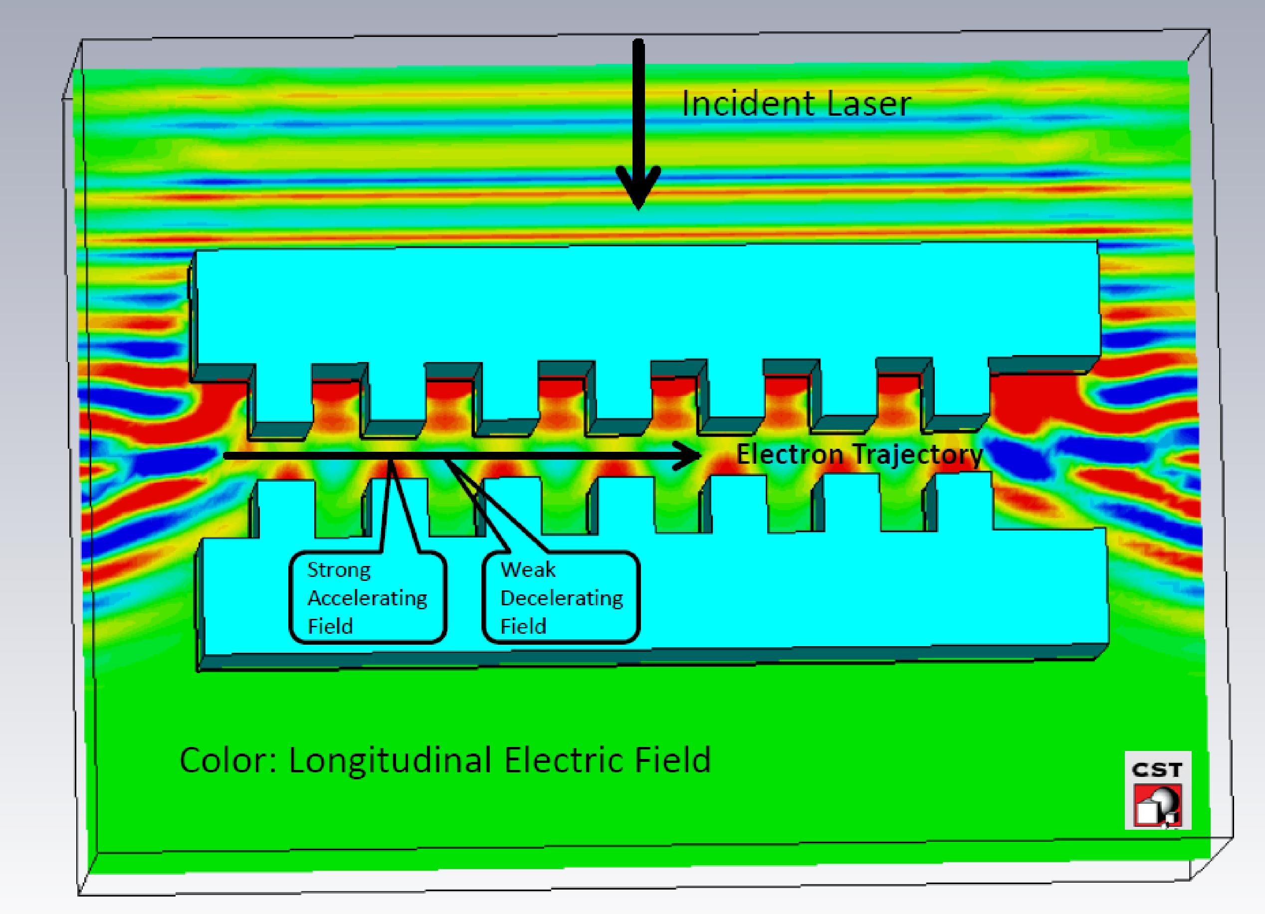
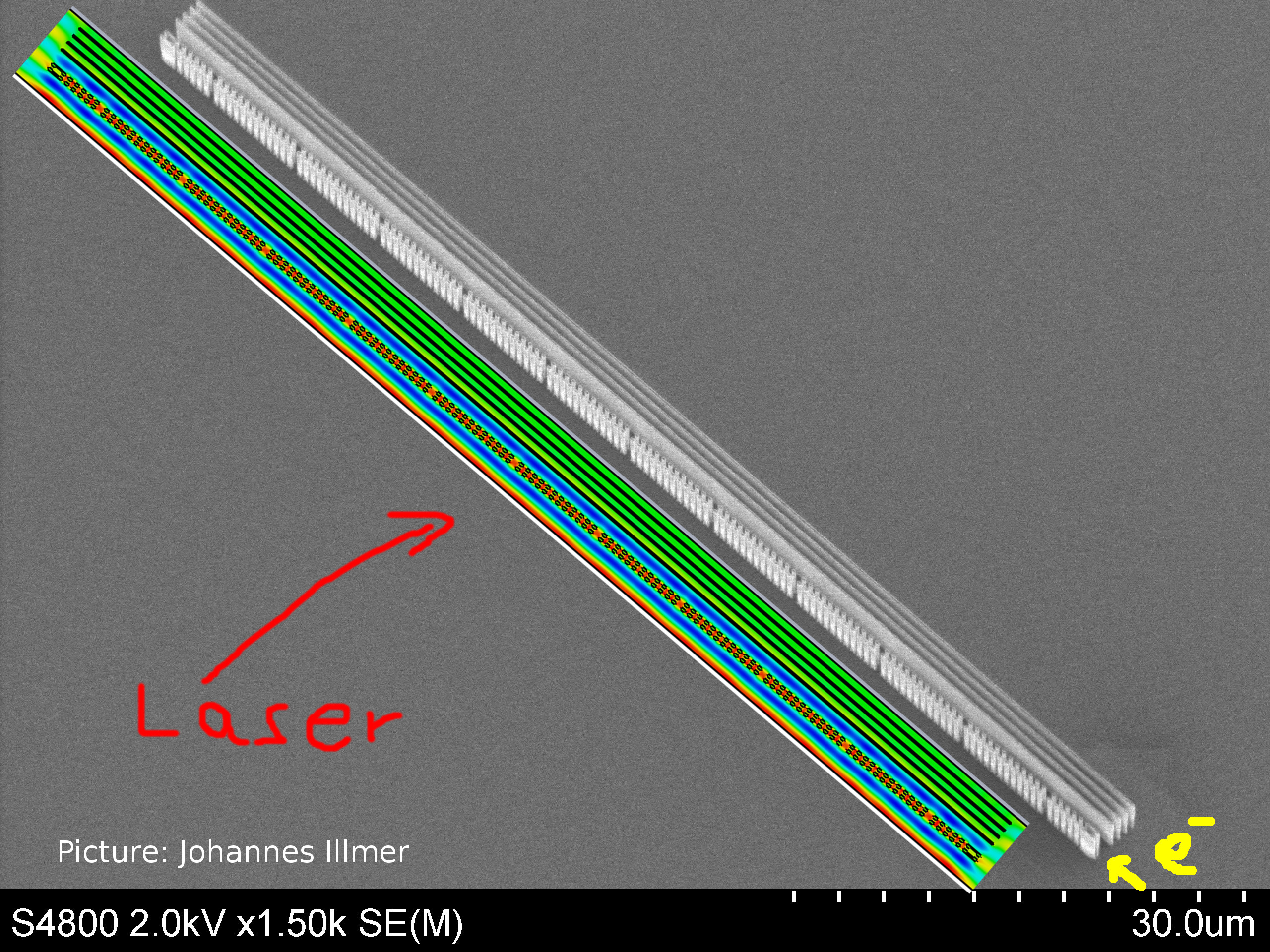
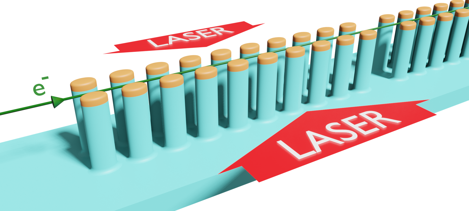
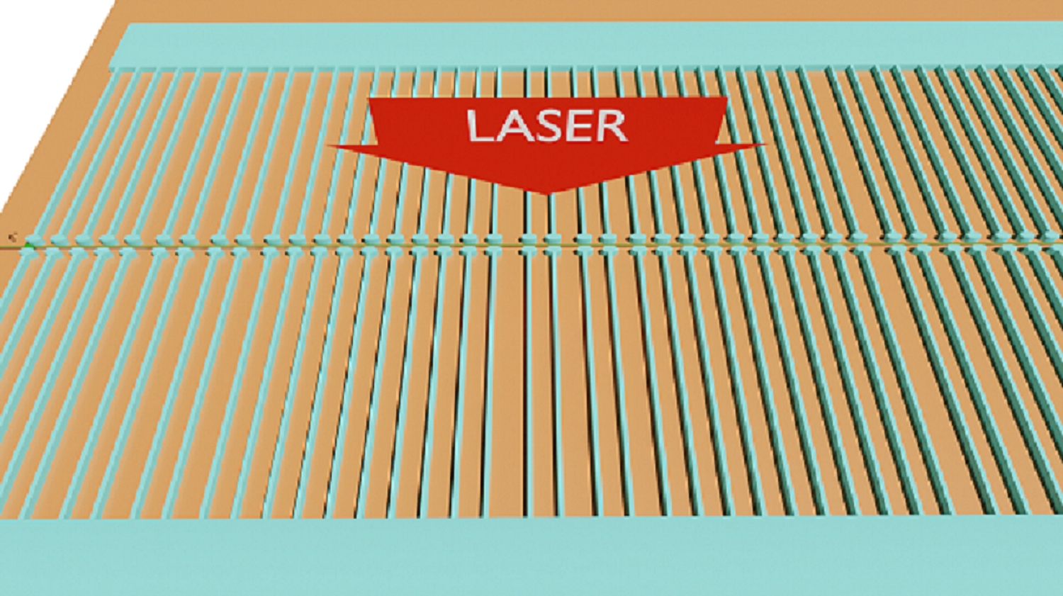
These structures function similarly to conventional Wideroe linear accelerators, except that the frequency is scaled from several hundred megahertz to several hundred terahertz (visible or infrared spectral range). This results in a corresponding reduction of the structure into the micrometre range (see picture). With the help of the grating teeth in the structure, the electric (near) fields are shaped such that a particle arriving at the right time experiences a strong acceleration close to the tooth. In the space between the teeth, the particle is only very slightly slowed down, which corresponds to a drift tube. All in all, you get a net acceleration. A very clear description can be found in this YouTube video.
The advantage of DLAs is that field strengths of >1GV/m can be generated with modern laser systems, which are already commercially available. Furthermore, dielectrics can also withstand significantly higher field strengths (breakdown-limit) than metals. Modern microfabrication technology, known from semiconductor technology, allows accelerator structures to be produced on a chip.
In order to develop a practical accelerator system, however, there are still some hurdles to overcome, which are defined in particular by the electron beam parameters. Due to the fact that only the near fields contribute to the acceleration, the aperture must be very small (~1µm). Furthermore, the time length of the accelerating edge is also only about 1fs, i.e. for an effective acceleration process, the beam must be bunched on this time scale. Our research is now focused on increasing the beam intensities in DLA experiments, which are still very low due to these limitations.
Since October 2015, our research group has been part of the ACHIP collaboration funded by the Gordon and Betty Moore Foundation, which has the goal of implementing an accelerator on a nanophotonic chip. The task of our group in the collaboration is both the field simulation and the simulation of particle dynamics in dielectric accelerator structures. This includes pure tracking simulations to determine the usable aperture as well as self-consistent particle-in-cell (PIC) simulations to quantify intensity effects. Furthermore, we particularly develop laser-driven focusing structures, which are crucial for the transport of non-relativistic electron beams.
ACHIP in the university newspaper hoch3 Forschen
The winter 2020 issue of hoch3 Forschen published the article “Particle accelerator in pocket format” about the ACHIP programme (german only).
Electron beam dynamics
To obtain a length-scalable accelerator on the chip, the electron beam must be held in a focusing channel. Since only the near fields can be used for acceleration, this channel is so small that conventional focusing methods, such as quadrupole magnets, would have to be extremely strong to prevent the electrons from colliding with the accelerating structures. This cannot be realized in practice by magnets. However, the laser fields themselves provide a means of exerting strong transverse forces on the electrons. To exploit this, the “Alternating Phase Focusing” (APF) technique known from conventional heavy-ion accelerator technology was applied to DLA. By combining the periodic structures into blocks with well-defined phase jumps in between, a quasi-periodic “focusing lattice” can be designed similar as for conventional accelerators, only miniaturized on the chip and driven exclusively by the laser. We developed the method first in a two-dimensional and then in a three-dimensional sense.
The 3D APF method allows to capture the electron beam also in the vertical direction, which enables full length scalability of the accelerator. Recently, the structures required for 3D APF have been designed for fabrication on so-called silicon-on-insulator (SOI) chips using a standard nanophotonics process. The vertically illuminated 3D APF on SOI structures required for a fully length-scalable accelerator on chip have been filed as a patent application. Vertical laser illumination of the accelerator chips makes the experimental setup significantly simpler since symmetric fields can be straightforwardly obtained on SOI wafers, Since highest lateral and longitudinal accuracy are intrinsically achieved by the lithographic process, only vertical corrections of the electron beam direction are required.
A complete electron accelerator on the chip thus only requires vertical correctors, which can be implemented with electrostatic deflectors directly on the SOI chip. For this purpose, a second wafer can be attached from the top (see picture).
This chip is designed in such a way that in each stage the energy of the electrons is approximately doubled. Thus, in about 4-5 stages one reaches from below 100keV to 1 MeV and beyond. The applications of such a chip are especially in ultrafast electron diffraction and so-called pump-probe experiments, which benefit from the intrinsic attosecond time scale of the DLA electron pulses and could in the future be performed with boosted energies at low cost in any university laser laboratory.